欧莱新材材料研究院
欧莱新材材料研究院共设立了6个市级、省部级科研平台和9个内设研发机构,拥有多名国内外具有先进行业经验的高端人才,研究课题涉及先进铜材料、靶材制备技术、半导体电子材料、薄膜技术、新能源材料(光伏电池、动力电池)、高纯金属、稀散金属、检测分析技术等领域,致力于打造产研用一体化的企业研发创新体系。
6个科研平台
市级、省部级科研平台
高端人才团队
国内外具有先进行业经验的高端人才
9个研发机构
内设研发机构,覆盖全产业链
核心研发设备
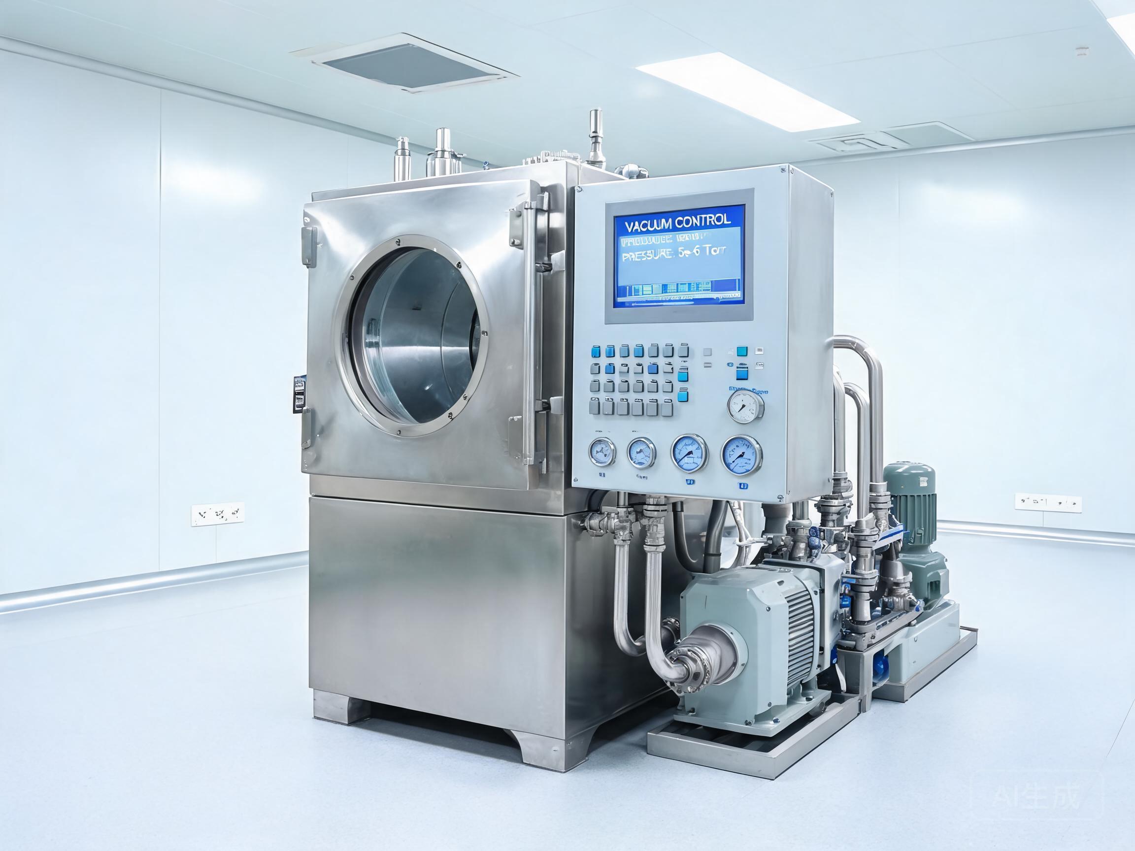
Core equipment for target sputtering verification, used in sputtering thin-film deposition process research.
Ultimate vacuum
≤5.0×10⁻⁶Pa
Sputtering power
DC/RF 500W
Substrate size
≤4 inch
Temp. range
RT-800°C
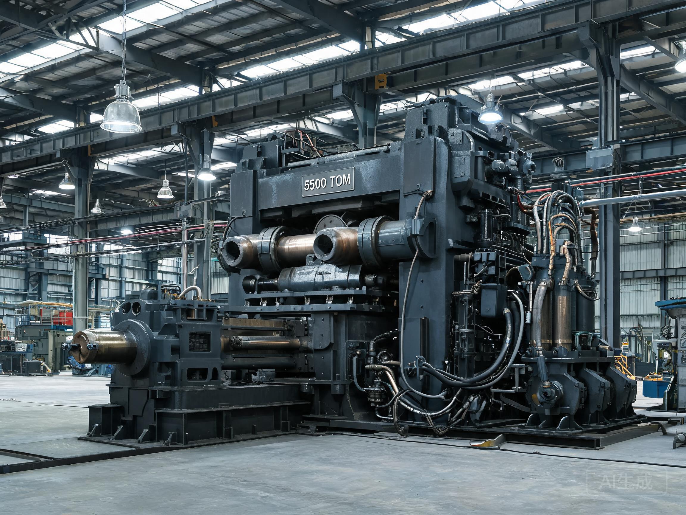
One of the largest dual-action copper extruders in the domestic industry, located at the Yuyuan production base, providing strong processing capacity for high-end copper alloy materials.
Rated pressure
5500 t
Container diameter
Φ280-420 mm
Extrusion ratio
up to 50:1
Product length
≤25 m
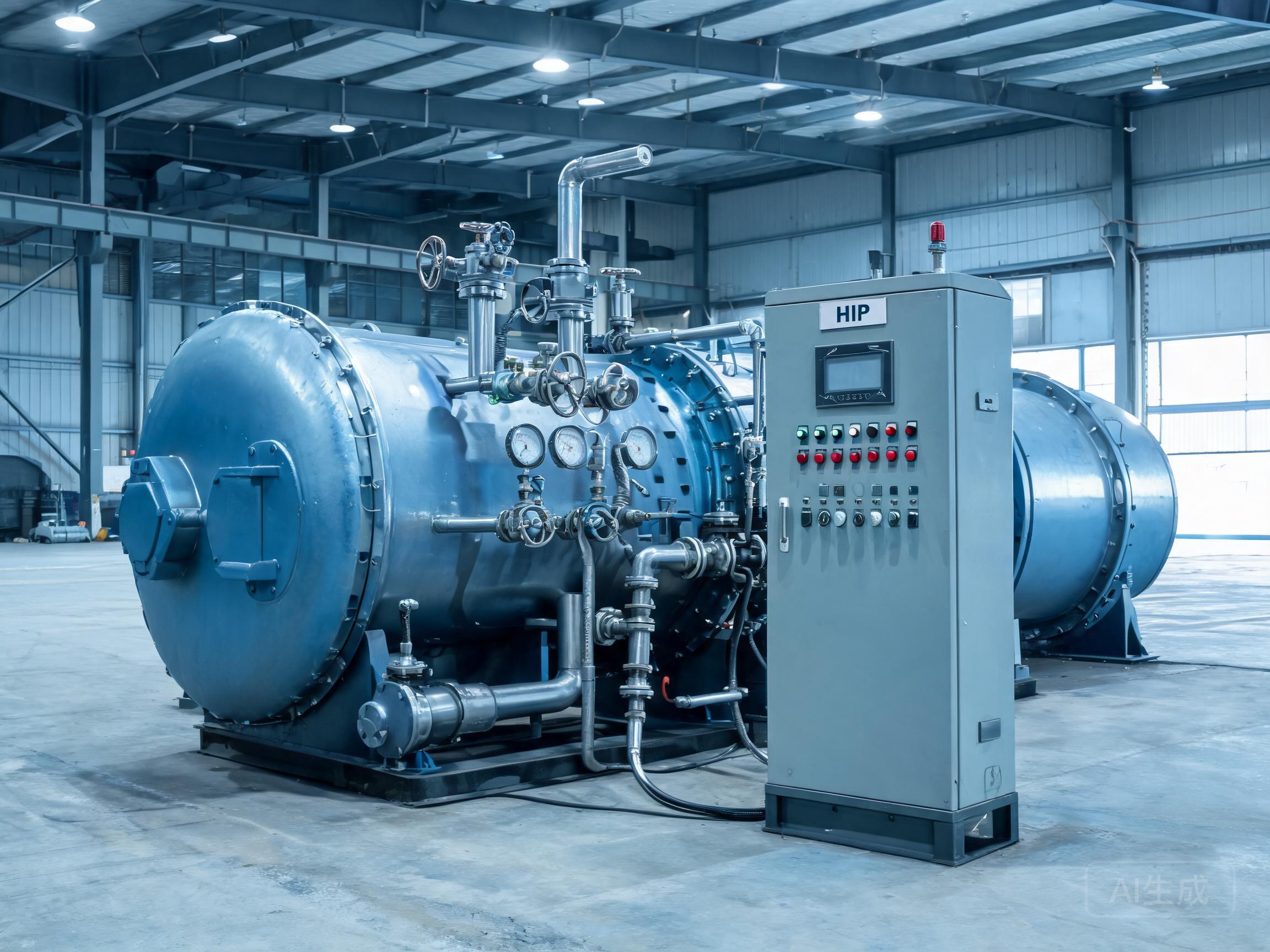
The largest hot isostatic press in South China, providing densification treatment for high-performance metals and frontier tech materials.
Max. temperature
1400°C
Max. pressure
200 MPa
Working zone
Φ500×1000 mm
Temp. uniformity
±5°C
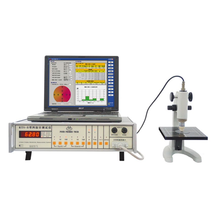
Accurately measures thin-film conductivity, suitable for resistivity testing of targets, metal films and other materials.
Resistivity range
10⁻⁵~10⁵ Ω·cm
Sheet resistance
10⁻³~10⁶ Ω/□
Measurement accuracy
±0.5%
Probe spacing
1.0 mm
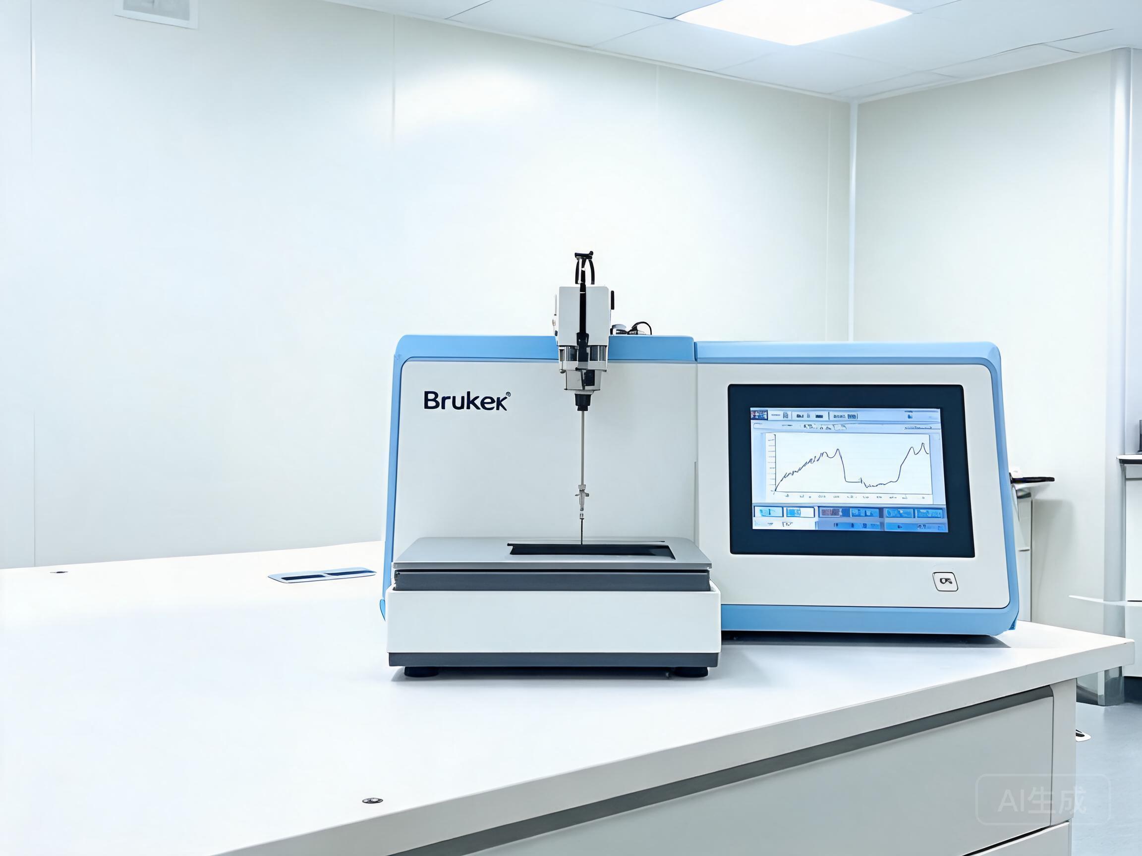
Nano-scale surface precision inspection, used for film thickness, surface roughness and other morphology parameter measurements.
Vertical resolution
≤0.1 nm
Scan range
≤50 mm
Max. sample thickness
50 mm
Stage size
200×200 mm
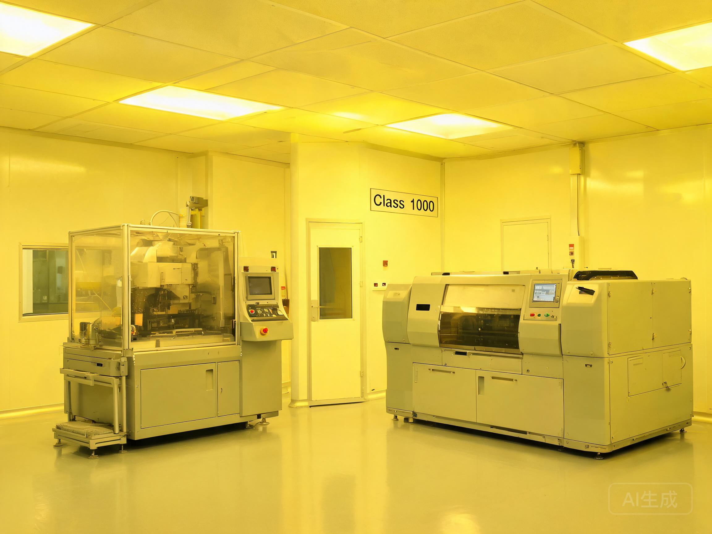
Semiconductor-grade clean environment equipped with lithography and development equipment, used for photolithography process R&D.
Cleanliness class
Class 1000
Lithography resolution
≤1 μm
Exposure area
≤6 inch
Overlay accuracy
≤0.3 μm

Used for micro-morphology observation and composition analysis of materials, with resolution down to nanometer scale.
SE resolution
≤3.0 nm @30 kV
Magnification
7X~1,000,000X
Accelerating voltage
200 V~30 kV
EDS analysis
B-U elements
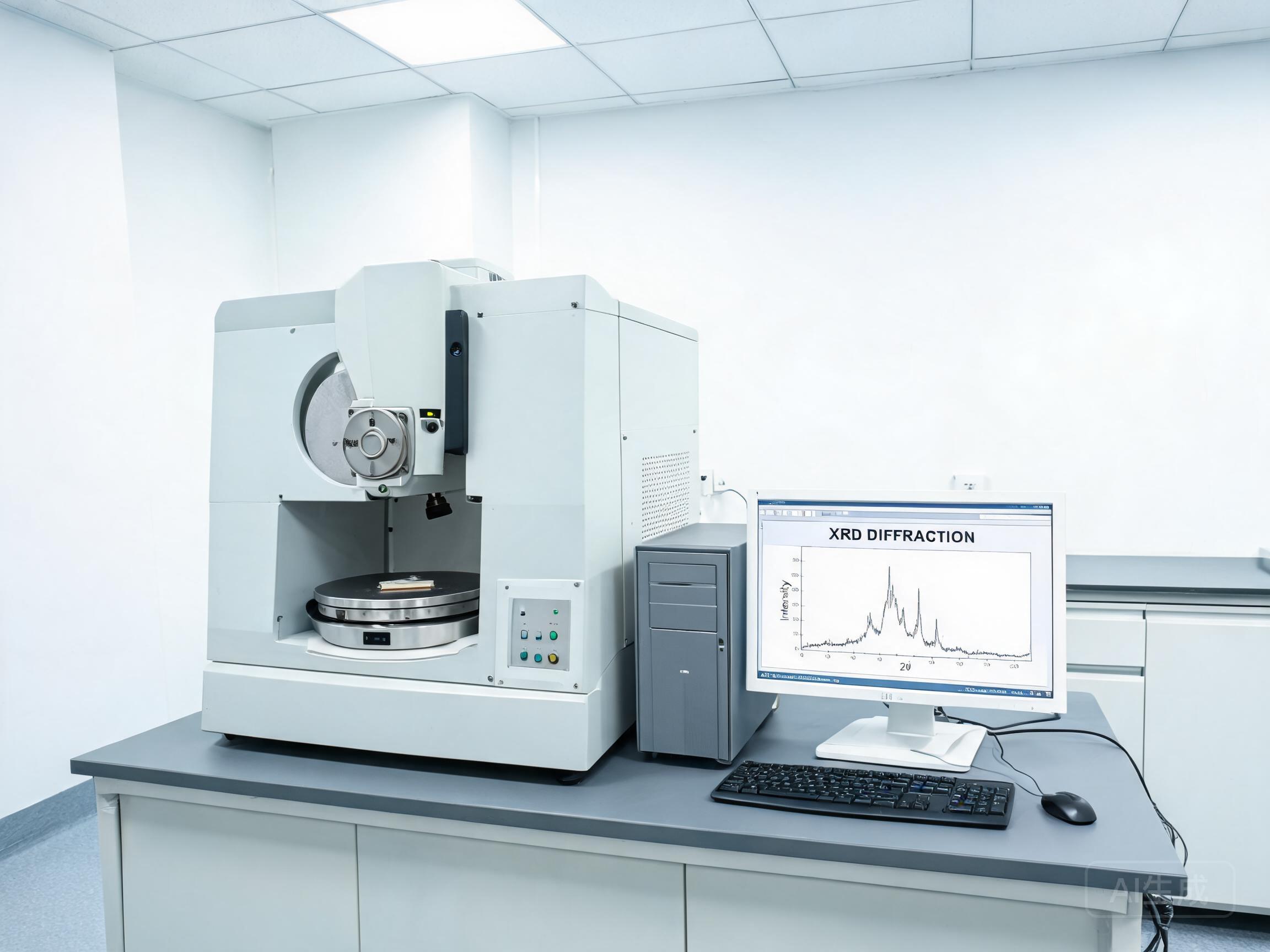
Qualitative and quantitative phase analysis of materials, used for crystal structure characterization of targets, thin films and other materials.
Angle range
5°~140° (2θ)
Measurement accuracy
±0.01°
X-ray source
Cu Kα
Max. power
3 kW
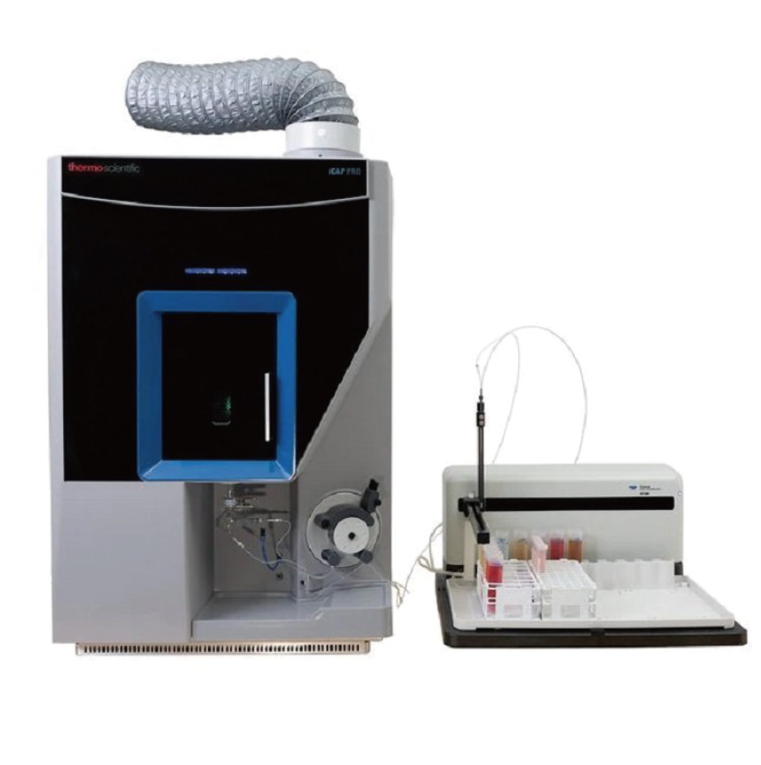
Inductively coupled plasma optical emission spectrometer, used for elemental content analysis in materials.
Wavelength range
167-852 nm
Analysis accuracy
ppm level
Detection limit
ppb level
Linear range
5-6 orders of magnitude
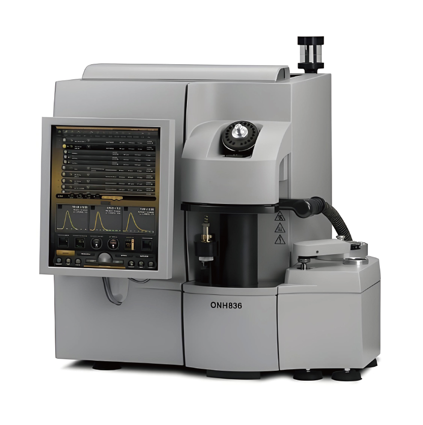
Accurately determines oxygen, nitrogen and hydrogen content in metal materials.
O detection range
0.05ppm~5.0%
N detection range
0.05ppm~3.0%
H detection range
0.1ppm~0.25%
Detection limit
0.025ppm(O)
